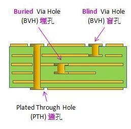
Common holes in printed circuit boards (PCBs) include through holes, blind holes, and buried holes.
Via (VIA), the copper foil line between the conductive patterns in different layers of the board is connected or connected by such holes, but it cannot insert the copper-plated holes of the component legs or other reinforcing materials. Printed circuit boards (PCBs) are formed by a stack of many copper foil layers. The copper foil layers cannot communicate with each other because each layer of copper foil is covered with an insulating layer, so they need to be connected by vias for signal connection, so there is a Chinese via. The title.
The via hole of the circuit board must pass through the plug hole to meet the customer's needs. In the process of changing the traditional aluminum chip plug hole, the surface resistive soldering and plug hole of the circuit board are completed by using white net, which makes the production more stable and the quality is more reliable. It is more perfect to use. The vias help the circuits to be connected to each other. With the rapid development of the electronics industry, higher requirements are placed on the manufacturing process and surface mount technology of printed circuit boards (PCBs). The plug hole process of the via hole is born, and the following requirements must also be met: 1. Only copper is needed in the hole, the solder resist can be plugged or not; 2. There must be tin lead in the hole, there is a certain Thickness requirement (4um), to prevent soldering ink from entering the hole, causing the solder ball to be hidden in the hole; 3. The through hole must have a soldering ink plug hole, opaque, no tin ring and tin bead, and must be leveled.
The blind via is to connect the outermost circuit in the printed circuit board (PCB) with the adjacent inner layer by using a plated hole. Since it cannot be seen, it is called a blind pass. In order to increase the space utilization between the board circuit layers, blind holes come in handy. The blind hole is also a via hole to the surface of the printed board.